Dice Game on a CPLD
A complex programmable logic device (CPLD) is a device which uses macrocells in order to implement logical functions. We took up this project as a way to understand the flow of taking a real world problem from the stage of hardware design, it’s implementation using a hardware description language and finally, the porting to a real hardware. This project was done by me and Manan at CEDT, NSIT under Prof. Dhananjay Gadre.
We were provided by a kit called PalDuino, which is a CPLD version of Arduino. It has the capability of programming via JTAG and pinheads in order to mount peripherals.
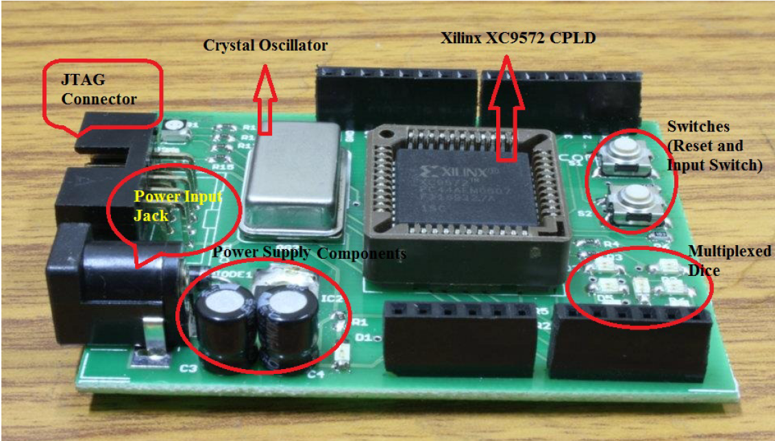
The shield looked like this, mounted on top of Palduino.
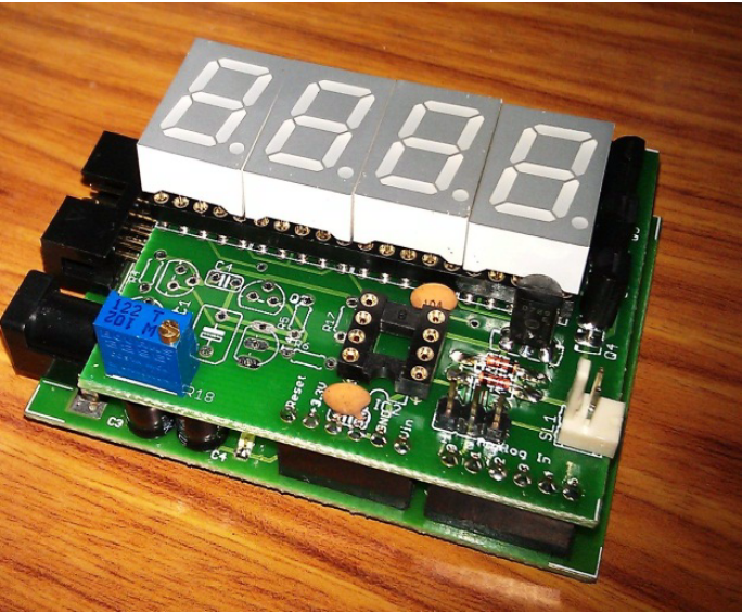
We got all this ready-made, thanks to the seniors in the lab. We were all set to write the VHDL now. It was only after a few days of struggling to make things work that we realized how important it is to use a modular approach. The most crucial point in defining an FSM is thinking of what the states should be. Once you have defined what the states are, the rest of the FSM is a piece of cake. Whether you’re trying to model the operation in a Moore or a Mealy Machine, the definition of the states is the most crucial step.
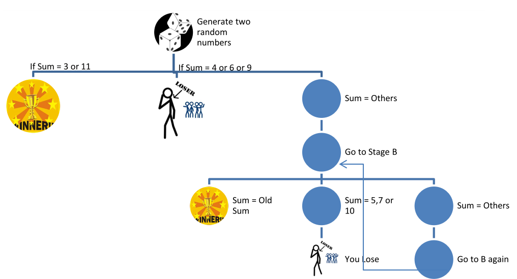
The game is rather simple. We took a few defined rules to define when a user would win/lose. It can be summarized using the following diagram:
The Seven Segment Displays (SSDs) were multiplexed with a common data bus and transistors connected to enable the SSDs separately. Only one of the SSDs should be enabled at one time so as to display the desired data. The data is switched each time before the next SSD is turned on. This takes place at such a rapid rate so as to create an effect such that all the SSDs are displaying data simultaneously. Therefore, two FSMs had to be implemented. Firstly, an FSM for controlling the SSDs. Two of the SSDs showed the number generated by the two dice and one of the other two used three segments to indicate whether a player Won, Lost or needs to Play Again.
The first FSM had to take an input data and mutliplex the SSDs to show the same. Following diagram shows this FSM:
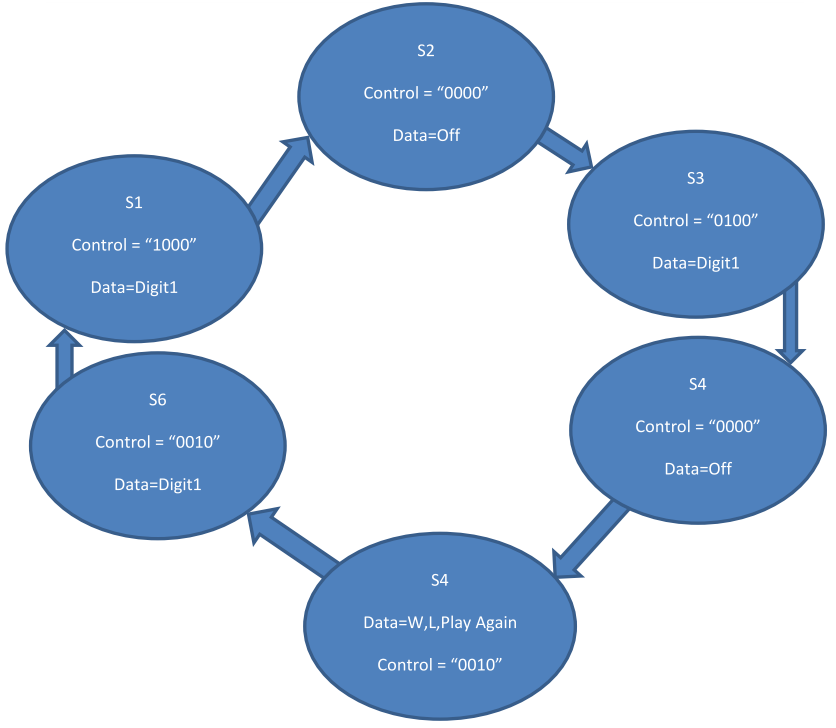
There are a few typos in the diagram. In S3, Data = Digit2 and in S6, Data = Off.
The other FSM denotes the game control. It might be a little hard to understand but I recommend trying to make it yourself and comparing afterwards. Following is the diagram for the same:
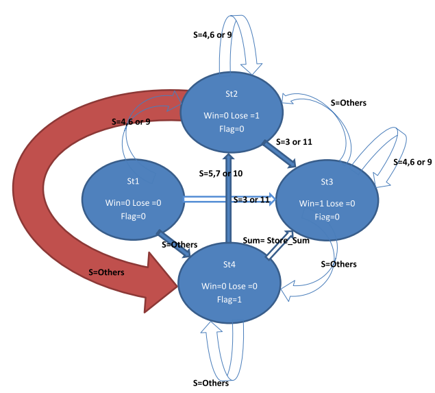
Both the FSMs are of Moore Type.
The major challenge in the project was to figure out all the pieces of the puzzle. The game control and VHDL is easy once the states are defined well. The multiplexing took a little effort to be up since the data display stages had to be interjected with “Data Off” stages to prevent data of one SSD from going into another.
After this you can load the constraints in the UPF file according to the hardware and burn away to get your Dice Game working. The VHDL Code is attached here.